

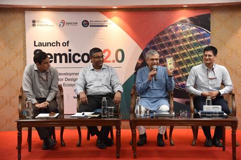
New Delhi, Aug 31: The government on Monday notified all six pillars of Semicon 2.0, seeking to expand India’s semiconductor capabilities across chip design, manufacturing, packaging, equipment, research and talent development, Union Electronics and IT Minister Ashwini Vaishnaw said.
Addressing the media, Vaishnaw said India had developed 85,000 semiconductor engineers in just four years, achieving in four years a target originally set for a decade. The government has now set a target of developing another one lakh semiconductor engineers, he said.
The minister also said India could account for close to 10% of the global semiconductor industry’s market in the coming years. Students from Tier-II and Tier-III cities have already designed more than 250 semiconductor chips, highlighting the widening talent base for the sector.
Semicon 2.0 builds on the first Semicon India Programme and will provide fiscal and infrastructure support across the semiconductor value chain. Its six pillars cover chip design; machines and materials; new fabrication plants; ATMP/OSAT packaging and testing; advanced semiconductor R&D; and talent development.
The scheme covers 10 categories, including semiconductor IP and system-on-chip design, wafer and compound-semiconductor fabs, display fabs, semiconductor manufacturing equipment and materials, and advanced technology research.
Projects supported under the scheme will generally run for up to six years, while applications will initially remain open for three years. The India Semiconductor Mission (ISM) will serve as the nodal agency, handling applications, appraisal and implementation oversight.
Vaishnaw said the emerging ecosystem is expected to generate 50,000-60,000 direct jobs. He also highlighted faster project execution, noting that commercial production began in one case within 13 months of groundbreaking, while approvals for various projects were secured in as little as 90 days.
The initiative is significant as India seeks to move beyond semiconductor assembly into design, fabrication and advanced technology, reducing supply-chain vulnerabilities while building a globally competitive chip industry.
